Technical portfolio, power electronics
Automotive grid-connected inverter design and application
A three-phase multilevel inverter for grid-connected vehicle applications, built to support emergency backup power, distributed energy from vehicle battery systems, and grid stabilization through power factor correction and reactive power compensation. Modeled and closed-loop controlled in MATLAB/Simulink, from PWM switching through dq synchronous-frame control, reactive power compensation, and PLL grid synchronization.
Three performance objectives
Grid-tied inverters enable several critical functions for vehicle-to-grid applications: emergency backup power when primary supplies fail, distributed energy generation from vehicle battery systems, and grid stabilization through power factor correction. The design parameters were optimized around three objectives.
Five design choices behind the performance targets
Each feature below was selected to move one of the three objectives, power factor, EMI, or THD, without trading away the others.
Lower switching frequency
Reduces the fundamental switching frequency to bring down EMI levels.
Multilevel topology
Mimics a more sinusoidal wave shape and reduces THD.
LCL filter
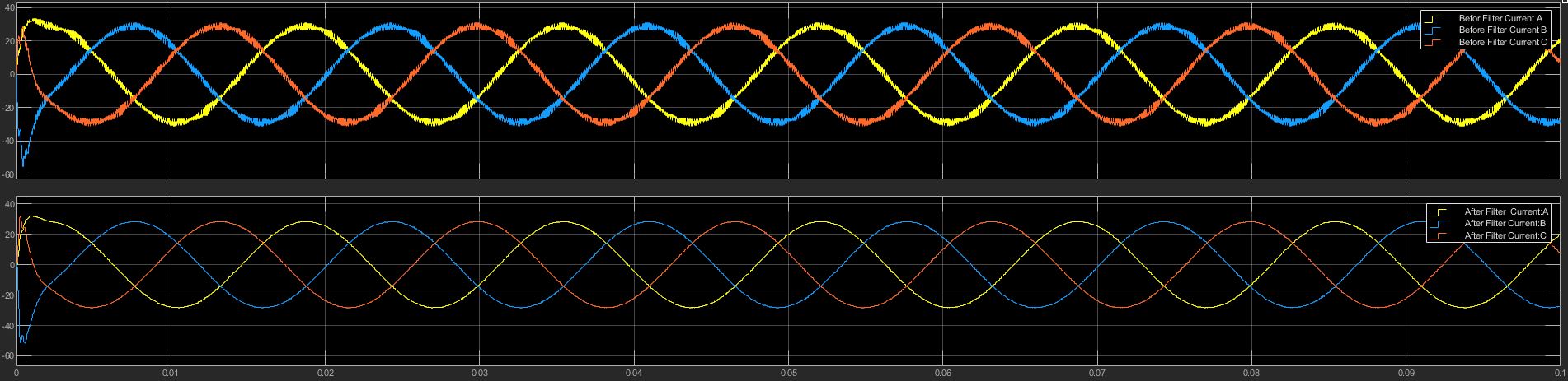
Smooths output current and increases power factor.
Tuned PID controllers
Commands accurate control schemes and minimizes losses.
Low RDS(on) MOSFETs
Minimizes conduction and switching losses at the device level.
Simulation and hardware specification
| Three-phase grid voltage | 480 Vrms |
| Fundamental frequency | 60 Hz |
| Baseline GCI topology | Three-phase two-level inverter, later moved to a nine-level multilevel design |
| DC-link voltage | 800 V |
| Switching frequency | 10 kHz |
| Sampling frequency | 2 MHz |
| Phase A angle | 0° |
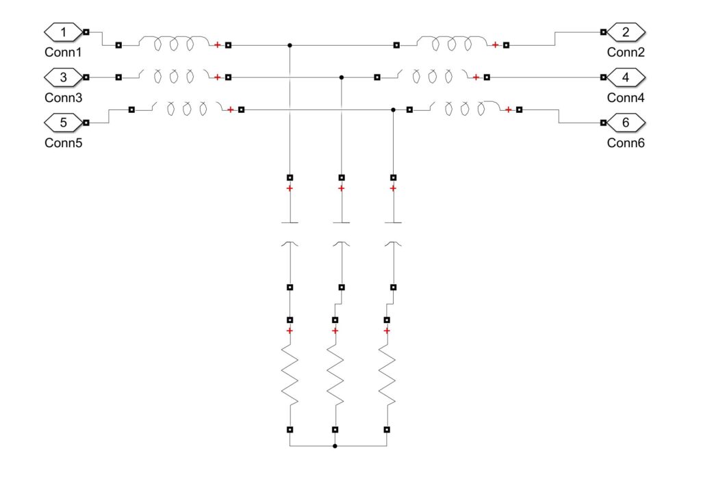
| Filter configuration | LCL filter |
| PWM scheme | Sinusoidal SVPWM |
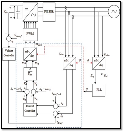
Closed-loop control, from PWM to power measurement
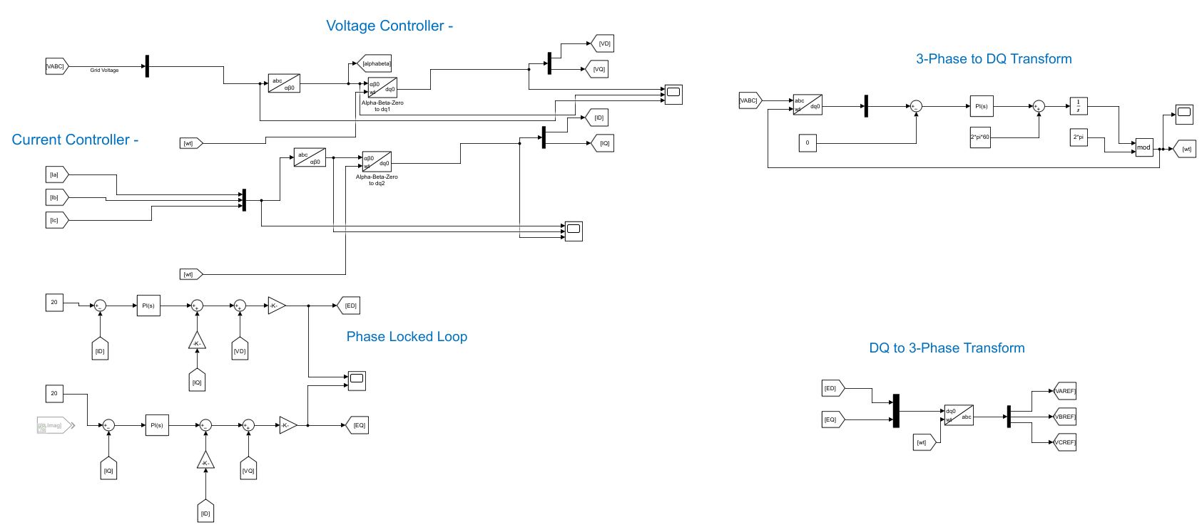
This is the complete closed-loop implementation behind the block diagram: grid source and LCL filter on the left, alpha-beta-zero to dq0 transforms feeding the voltage and current controllers, a discrete power-measurement block computing real and reactive power, and a THD block reading total harmonic distortion directly off the filtered output. The PI-based voltage and current controllers at bottom left generate the ED/EQ and reference sine waves that drive the PWM stage.
Grid source, LCL filter, and inverter stage
A cleaner view of the same signal path, isolating the three-phase grid source, the LCL filter stage, and the compressed inverter and DC power supply block that stands in for the switching bridge and controller output during power-stage validation.
Grid voltage and the inverter’s synchronized output
With a 480 Vrms grid, the peak line-to-line voltage works out to 480 × √2 = 678.82 V. Dividing by √3 gives the peak line-to-neutral voltage of 391.92 V, the reference the inverter’s own output has to track. The inverter’s artificial three-phase output is phase-locked to that grid reference using the PLL and dq control loop described above.
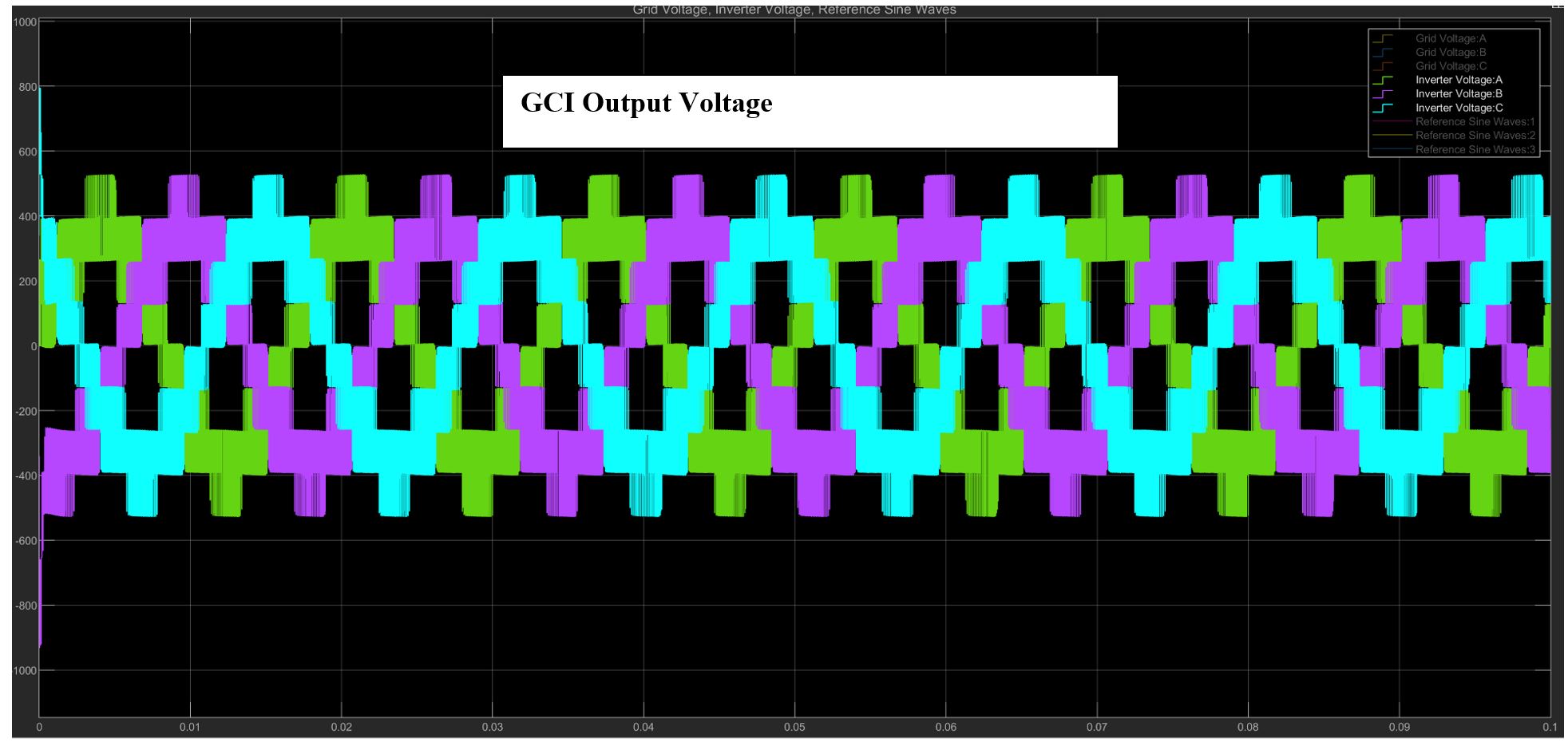
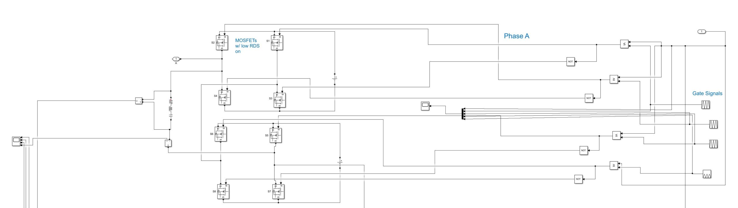
A cascaded nine-level sinusoidal output
As seen in both the output waveform and the inverter hardware design, this circuit creates a cascaded nine-level sinusoidal output. The added levels bring four concrete benefits:
- Elimination of low-order harmonics without an increase in high-order harmonics
- Lower total harmonic distortion
- Higher achievable voltage levels
- Less electrical stress on individual switches
Device-level efficiency
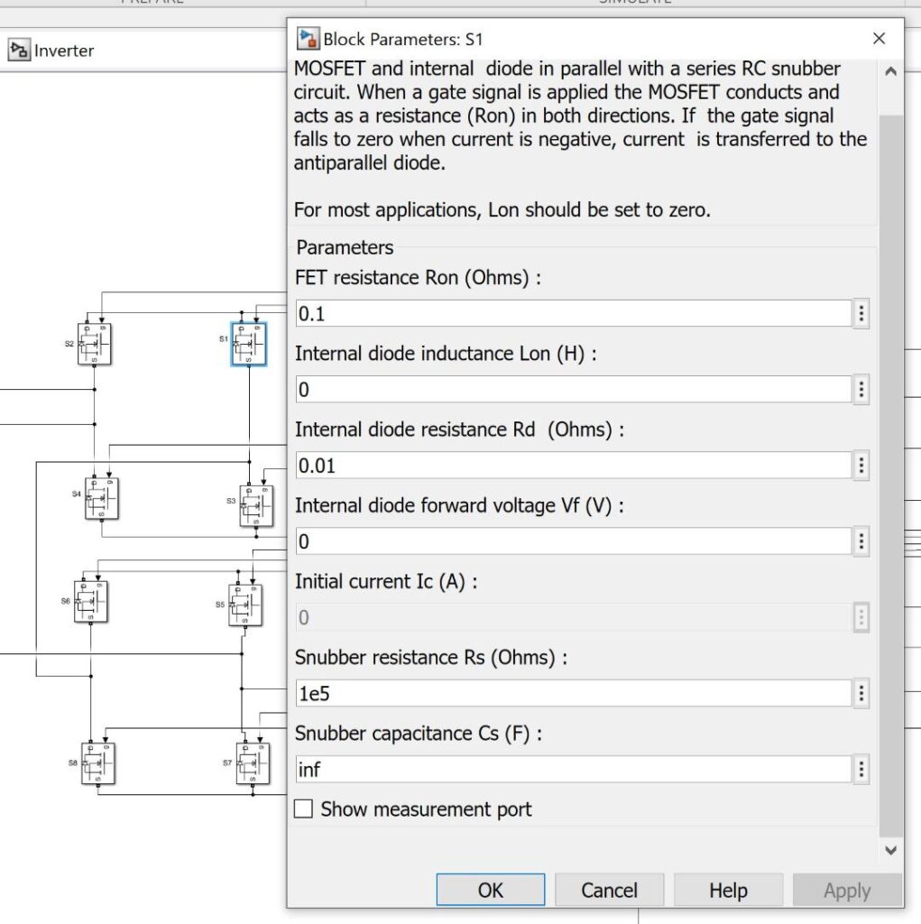
Alongside the multilevel topology, a low RDS(on) was considered for efficient inverter switching. One design consideration left out of this model is the gate resistor. Depending on the capacitance of the FET, the gate resistor can significantly affect switching speed, and with it both switching loss and EMI.
LCL filter: smoothing current, raising power factor
The comparison shows inverter current before and after the LCL filter was added to the circuit.
Voltage and current control, phase-locked to the grid
The phase-locked loop (PLL) adjusts the circuit’s output voltage to match the frequency of the reference signal, the grid frequency. The voltage and current controllers work in the dq synchronous frame, shown in the full implementation, to hold that lock under load.
Result: inverter output compared with the grid
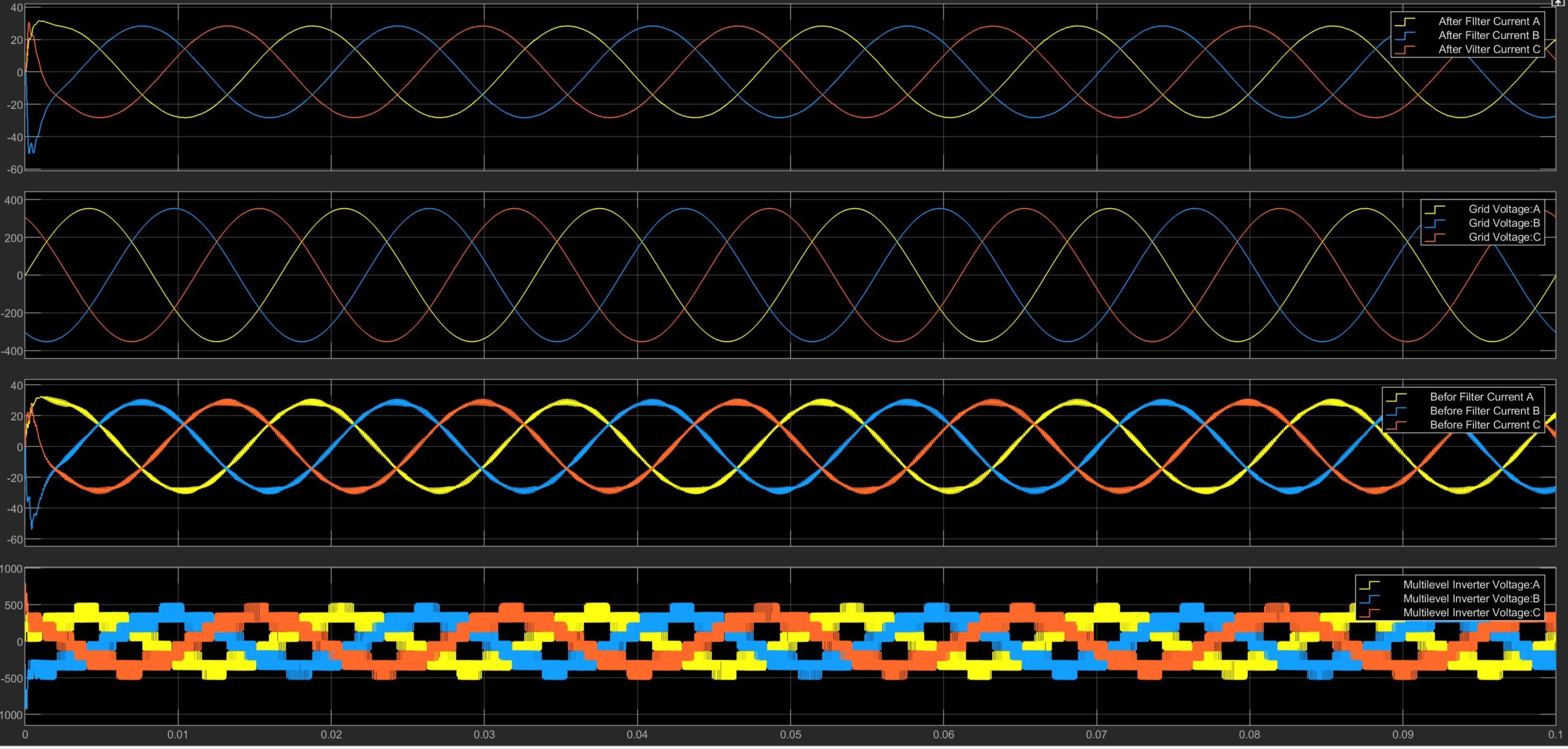
Between the inverter topology and the stepped output waveform, this design carries a multilevel, modular character that lets it better replicate a sinusoidal wave, holding sub-1% THD while staying synchronized to the grid it feeds.
Two-level versus multilevel: why the extra complexity was worth it
The original two-level design held THD around 1.5% even with the dq-PLL active. Moving to the multilevel topology brought THD under 1% and kept it there, even with current injected into the d- or q-axis, confirming that the added switch count was buying real distortion performance, not just complexity.
Reactive power compensation: closing the loop on an RL load
With a 5 Ω, 5 mH RL load added at the point of common coupling, the load’s own d- and q-axis current draw was measured. The GCI was then closed-loop controlled to supply the reactive component directly, so the grid only has to supply real power.
After compensation, the grid-side current amplitude drops and shifts back toward phase with the grid voltage, the signature of reactive power now being sourced locally by the inverter instead of pulled from the grid.
Grid voltage support: riding through a 10% sag
Adding grid impedance (Lgrid = 1.5 mH, Rgrid = 0.56 Ω) and reducing grid voltage by 10% reproduces a voltage sag event. From the reactive power required to correct that sag, the corresponding q-axis current command works out to roughly 127 A.
This is the same control loop used for reactive power compensation, redirected at a grid-support problem: instead of correcting a load’s power factor, the inverter now props up sagging grid voltage directly.
Engineering takeaway
A grid-connected inverter is a systems problem, not a single-component one.
Power factor, EMI, and THD pull against each other, and the fix for one is rarely free with respect to the other two. This design works through that tradeoff at every layer, topology, switching frequency, filtering, and control, to land on sub-1% THD while holding synchronization with the grid it is tied to.
Model developed and simulated in MATLAB/Simulink. Portfolio project by Brett Walker, Indianapolis, Indiana.