The following page will describe a three-phase two-level inverter for grid-connected vehicle applications. As mentioned on the home page a couple use cases of grid connected inverters involve powering commercial equipment when the primary power supply has been compromised, as well as providing secondary power from nontraditional sources such as automobiles, and grid power factor stability. Various parameters below have been altered in order to increase power factor, reduce EMI levels, and minimize THD.
-Lower fundamental switching frequency to reduce EMI Level
-Multi-Level inverter which mimics a more sinusoidal wave and reduces THD
-LCL Filter to smooth out current and increase power factor
-Tuned PID controllers that command accurate control schemes and minimize losses
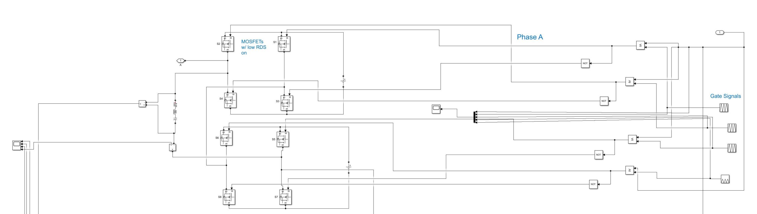
-MOSFETs with a low RDS ON to minimize switching losses
Model Parameters
Three-phase grid voltage = 480 Vrms
Fundamental frequency: 60 Hz
GCI Topology: Three-Phase Two-Level Inverter
DC-link voltage: 800 V
Switching frequency: 10 kHz
Sampling frequency: 2 MHz
Phase A angle at 0 degree
Filter configuration – LCL filter
PWM Scheme – Sinusoidal SVPWM
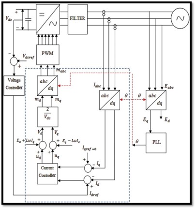
Block Diagram
Model of Grid Connected Inverter
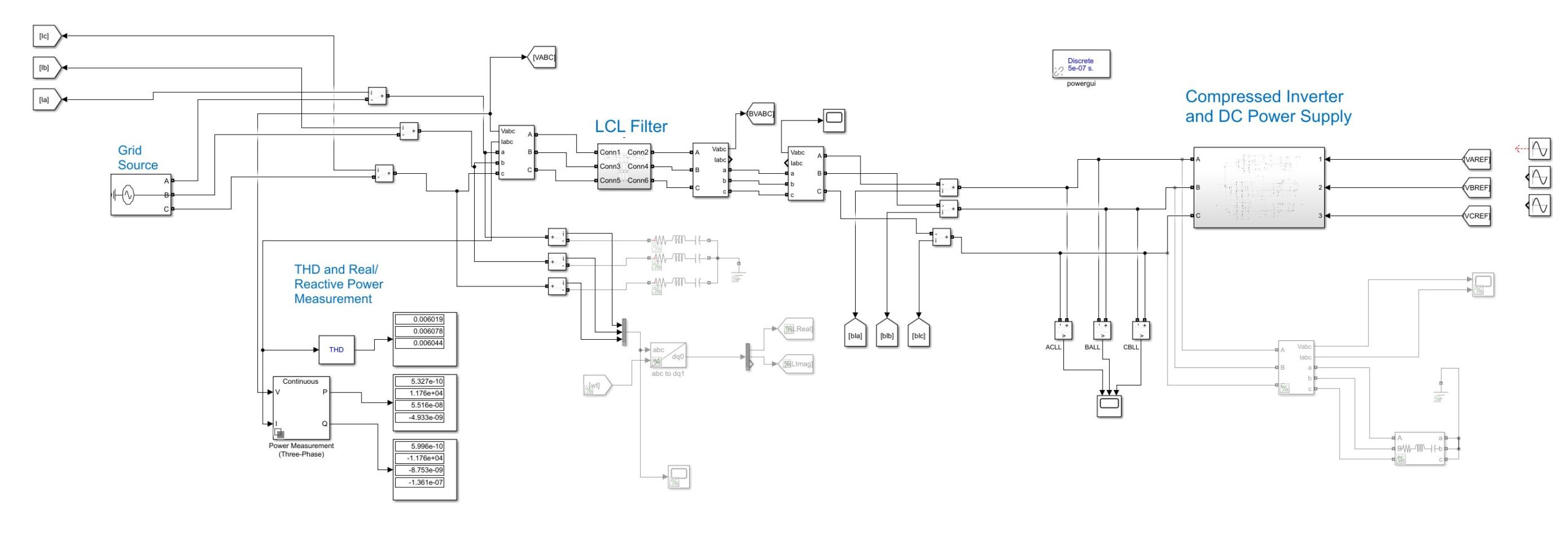
Above is a diagram of the full-scale grid connected inverter (GCI). Similar to the block diagram there are several key features within the GCI which allow it to invert a DC source into a 3-phase system while also syncing this artificial signal with the fundamental frequency of the grid.
Grid Output Voltage
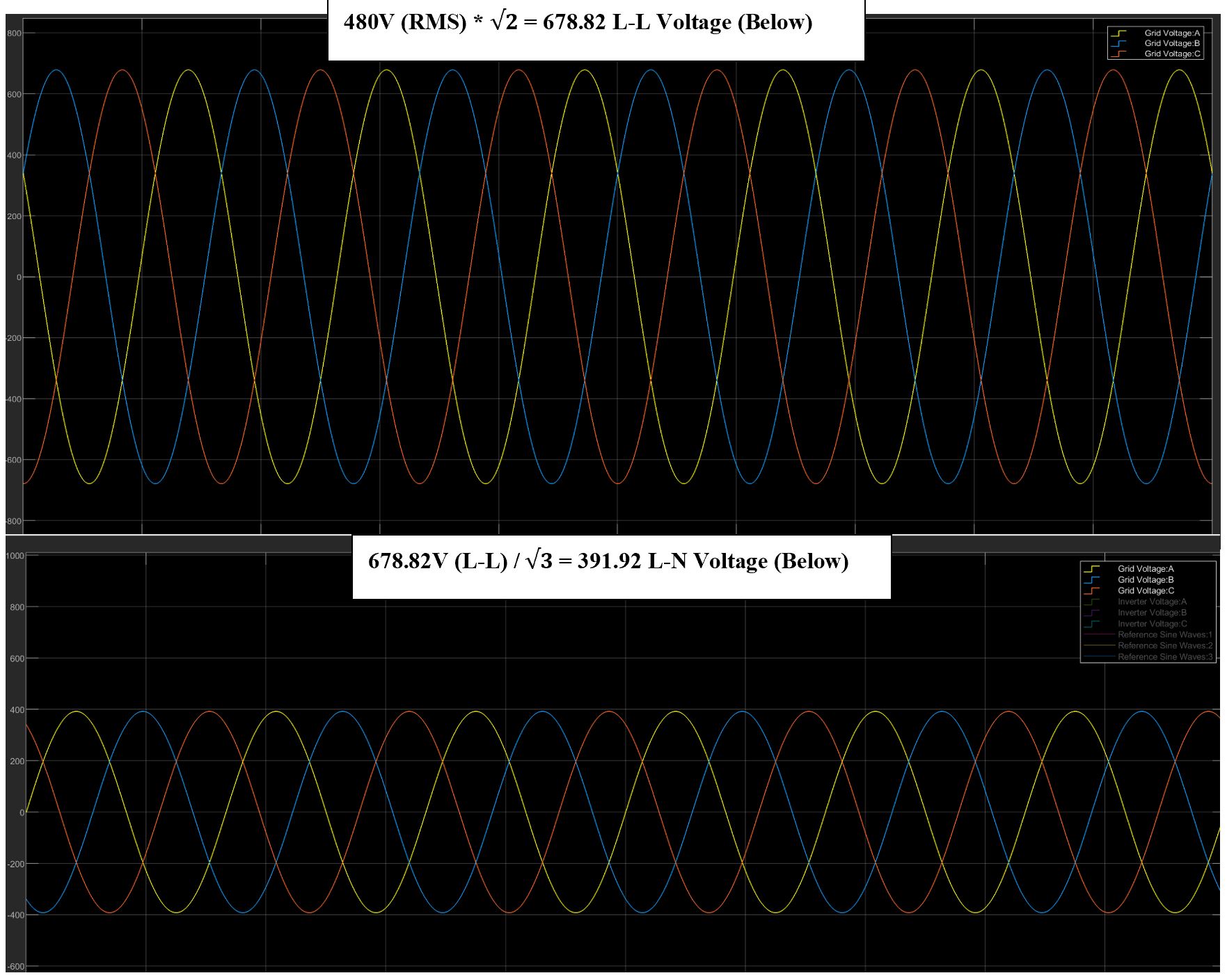
The Grid line to line (L-L) and line to neutral (L-N) voltages can be viewed above while the artificial GCI Output Voltage is displayed below.
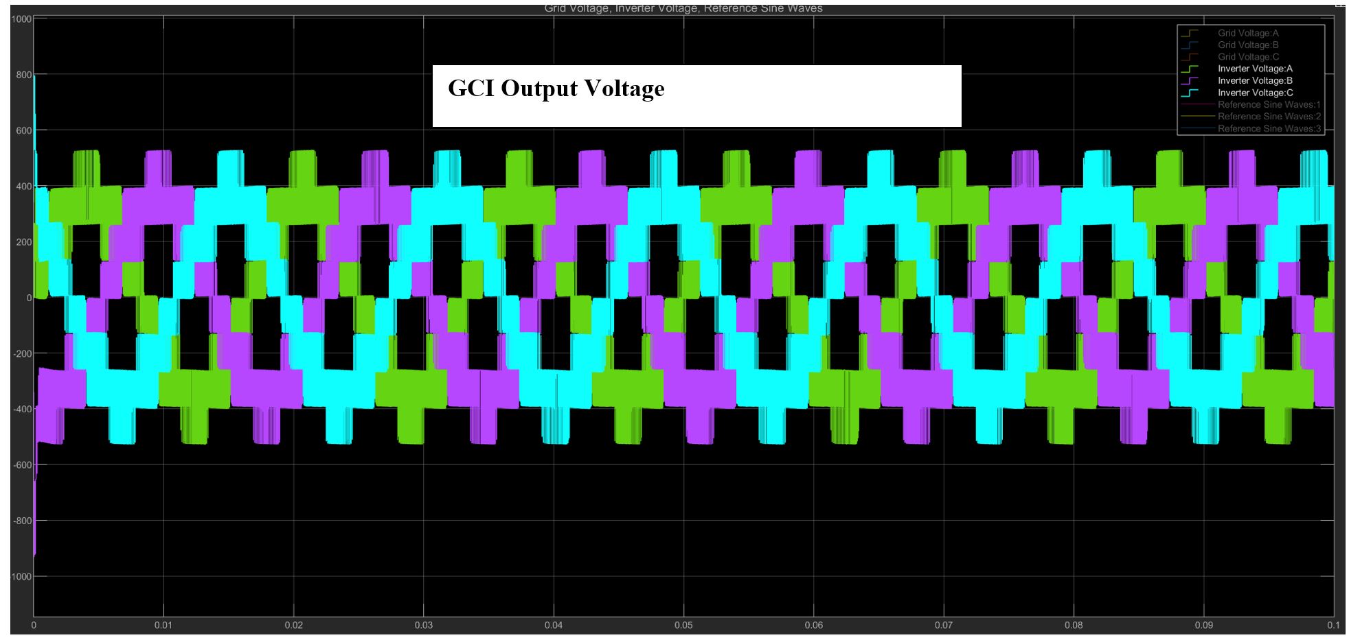
Let’s now examine the inverter topology capable of generating the above output voltage.
Modular Multilevel Inverter Design
As seen above in both the output wave plot and inverter hardware design this circuit creates a cascaded 9-level sinusoidal output. Benefits of the increased number of levels are below: – Elimination of low-order harmonics without the increase of high-order harmonics
– Lower total harmonic distortion
– Higher voltage levels
– Less stress on switches
FET Electrical Properties
Along with the multilevel topology a low RDS was also considered for efficient inverter switching. Another design consideration left out of the model would be the gate resistor as depending on the capacitance of the FET the gate resistor can greatly impact switching speed.
LCL Filter
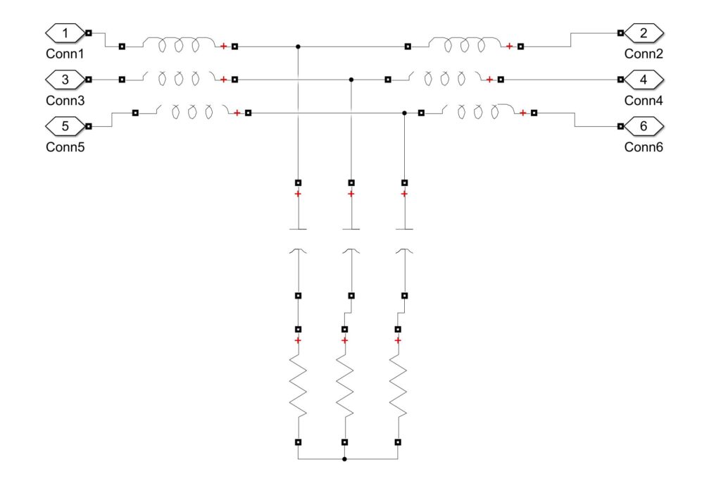
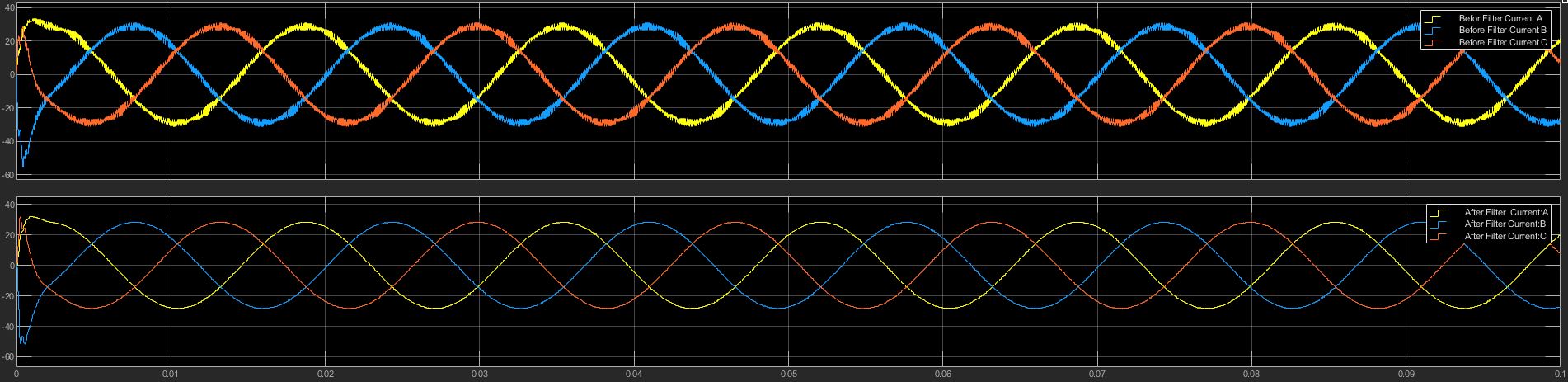
In the below output diagram, a comparison is made between the inverter current before and after a LCL filter was added to the circuit.
Voltage/Current Controllers and the PLL
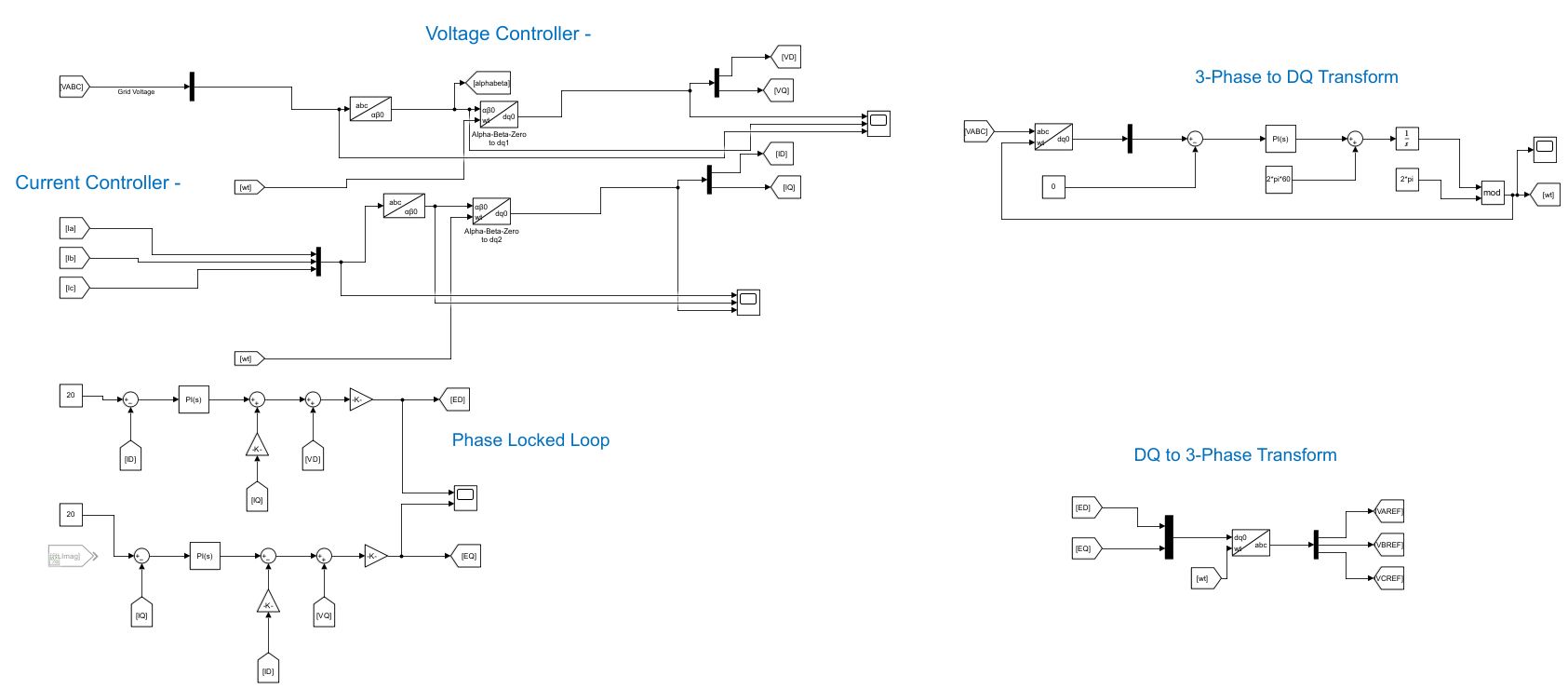
The Phase locked loop (PLL) modulates the electronic circuit output voltage to match the frequency of the reference signal (Grid Frequency).
Inverter Output compared with Grid
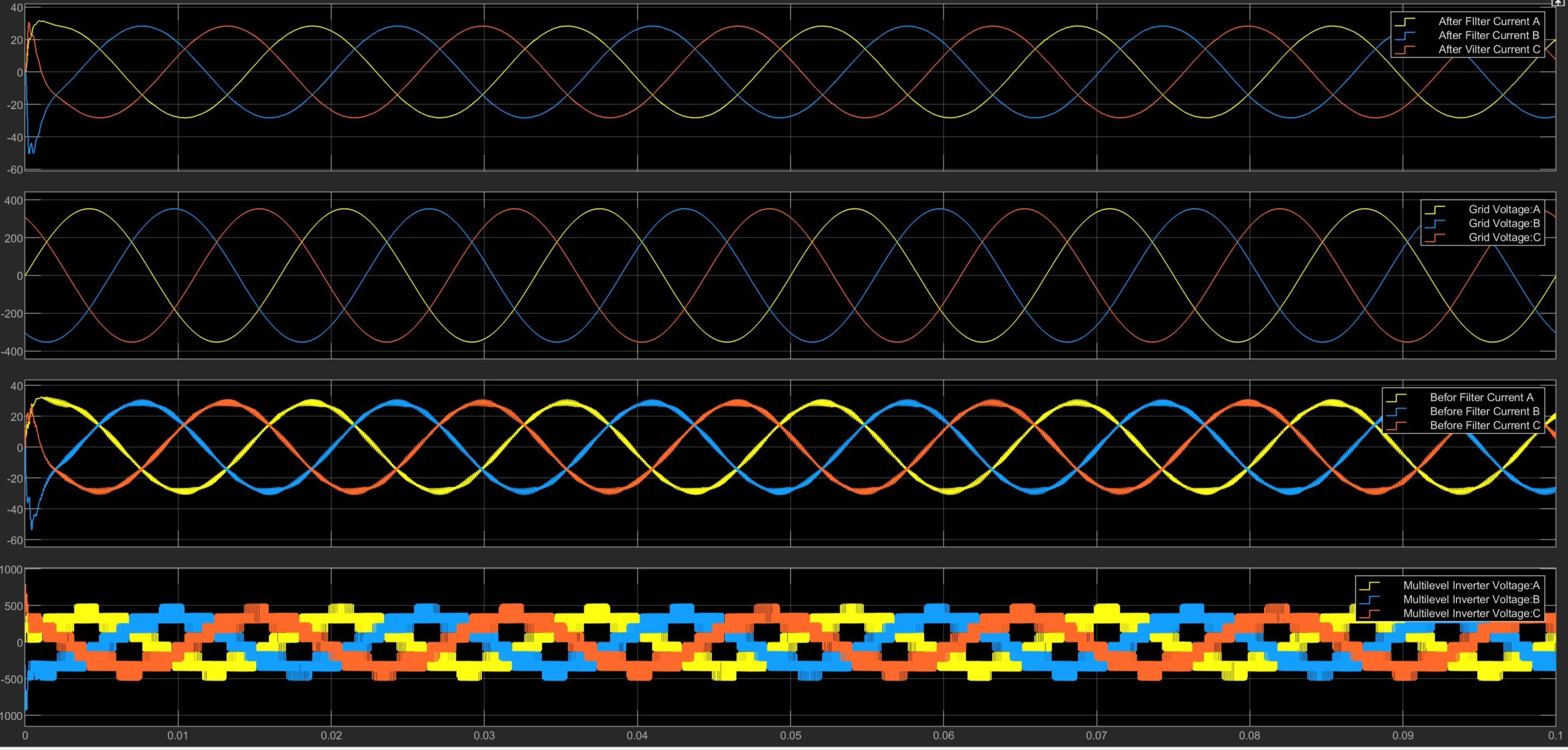
As seen in the by both the inverter topology and the stepped output waveform, this inverter has a multilevel modular theme which allows it to better replicate a sinusoidal wave.