Power supplies are an essential part of every electrical system deployed in the environment. It is critical for power supplies to be robust against electrical transients, and overstress as any power failure even if for a brief instance can result in an overall breakdown of the total system. As mentioned on the home page this schematic employs numerous design strategies to mitigate power supply failure. In order to confirm a product’s electrical resilience, the electronic system/component could be subjected to any of the following standards below:
- MIL-STD-1275 (Defense Transients → Over Voltage/Current and Reverse Battery Exposure)
- MIL-STD-461 (Defense EMC)
- ISO 7637 (Transients → Over Voltage/Current and Reverse Battery Exposure)
- IEC 61000-4-2 (ESD)
- IEC 61000-4-4 Transients
- IEC 61000-4-5 Surge Immunity
- GMW 3097 (GM specified ESD, Transients, and EMC)
- ISO 10605 (ESD)
- ISO 16750 (Transients)
- SAE J1113-13 (ESD)
- DO-160 (Aerospace Transients, ESD, and EMC)
Below is a diagram by Isaac Sibson of Diodes Incorporated on ISO-16750 Automotive Transients. As seen below these transients can manifest themselves in various forms, and it is important for the EE to understand the energy within the pulse and how to properly dissipate it.
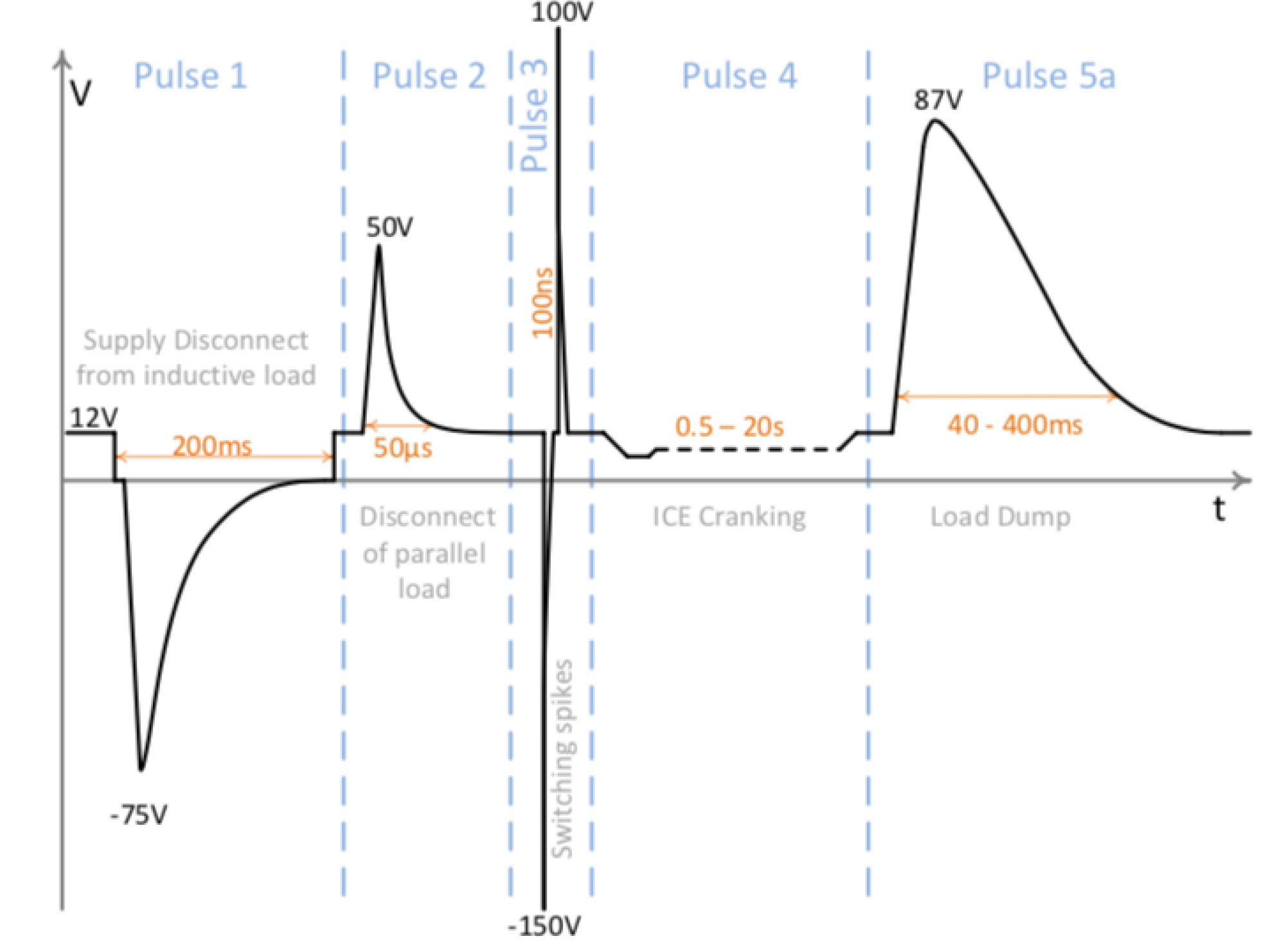
Through numerous tests and different methodology, the 8/20 or 10/10000 I_PP transient pulses were derived to represent typical industry transitory phenomena.
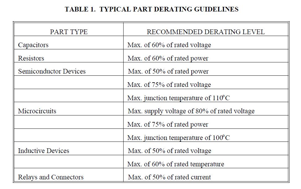
Another part of the design process and a guideline that should be referenced on all component selections is the safe operating area (SOA) and derating. Derating components allows for a margin of safety as power and temperature increase beyond nominal limits. Designing your circuit in alignment with a chart similar to the one below will allow for robustness to a variety of different environmental and electrical stimuli.
In an effort maintain the above chart then voltage, current, and temperature ratings protection circuits are instituted as mitigation efforts to avoid catastrophic failures. The maximum voltage level in this circuit is set at 32 Volts due to the parallel Zener diode. This diode will start to conduct when its reverse working voltage is met/exceeded and then will ultimately “clamp” the system to ground at its max rated clamping voltage/current. ————————EDIT. To ensure the system will not fail in the presence of negative voltage (Such as Reverse Battery Connection) the circuit includes design solutions that will protect the power supply. For example, the P-Channel FET is oriented so that its body diode will stop all negative voltages up to_______________________.
It is also a responsibility of the design engineer to protect the circuit from electromagnetic interference and ensure that the product complies with industry standards/specifications. Example electromagnetic compatibility (EMC) standards can be seen below:
- MIL-STD-461
- CISPR-25
- RTCA DO-160
To meet these standards a plethora of passive and active circuits are used to ensure IC clock frequencies and converter/inverter switching frequencies do not interfere with the outside world or other components in the nearby area.
PDNs, impedance matching, Bode Plots, and vector network analyzers
PCB Design
After component selection and circuit simulation I now move on to laying out a printed circuit board.
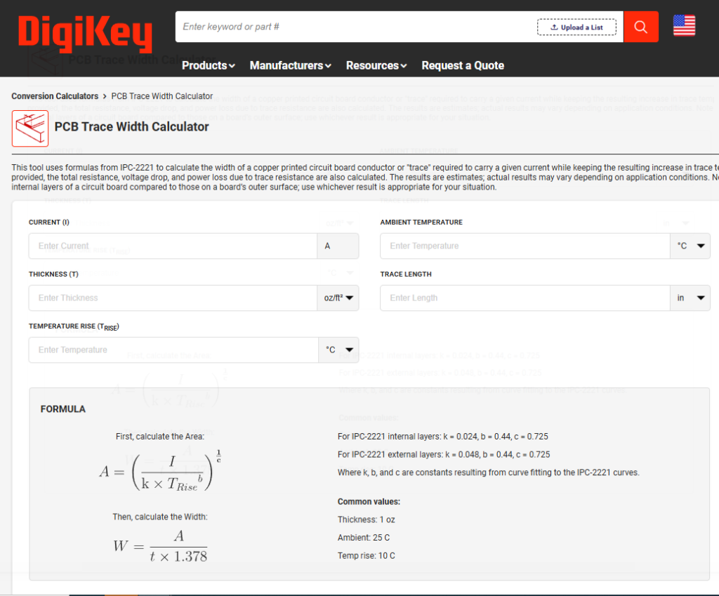
Trace Width Calculator